What is often missed in an automotive power supply when choosing an integrated circuit is not the specification on the data sheet but how the device will operate in the final design. This is because the datasheet covers the integrated circuit performance and can miss how the device will work in a closed loop or how it will interact with other components in the system. This is even more important when choosing a front-end power supply for an automotive design. The power supply that connects directly to the battery needs to offer high efficiency, small solution size and be very quiet. But why is this so?

TI’s new LM53635-Q1 regulator is more than a converter; it is also a power-conditioning circuit connecting the noisy and harsh environments of automotive electromechanical systems – such as the transmission, engine and braking – to highly sophisticated electronic control units (ECUs) using leading-edge processors and sensors that are susceptible to harsh conditions. The front-end power supply also has to manage fault and user conditions, like double battery or load dump. In this post, I will describe what you should consider when designing automotive power supplies and what additional functionality to add to your design to make the challenges more manageable. I’ll also be describing TI’s new 36-V, 2.1-MHz synchronous buck regulators.
A modern automobile includes many fuel-saving features; one of these is start-stop operation. Start-stop activates when the automobile rolls to a stop and the engine switches off to save fuel while in a traffic queue or waiting at a stoplight. Another condition called cold crank places similar electrical loads on the system. The cranking of the engine applies a large load to the system, causing a drop in battery voltage.
Under start stop or cold crank the voltage can drop quite dramatically – and to a level that causes the buck converter to go out of regulation. In some instances you may need to use a boost converter in the circuit to assist the system. If you design your power supply to support sudden voltage drops, it is possible to save the expense of the boost, as well as the cost, space and power consumption associated with the additional components.
A combination of close to 100 per cent duty cycle, very short minimum off-time and a low RDSON high-side field-effect transistor (FET) resistance enables the LM53635-Q1 (see Figure 1) to support deep drop of lower than 0.6Volt under full load and full operating temperature range whilst maintaining regulation for downstream power supplies without adding additional design complexity.

Figure 1: Dropout for the LM53635-Q1
Offering low electromagnetic interference (EMI) power supplies is becoming more important due to many factors, including the increasingly more complex wire harnesses used in automobiles and the number of ECU nodes being added to the system. Each harness wire and each ECU has the ability to create noise that can be transmitted around the automobile and affect other applications. Given the increasing number of safety applications, the ability to offer low EMI is highly desirable. TI used several techniques in the design of the LM53635-Q1 to minimise EMI.
One technique was to design the package layout for optimum placement and positioning of the passive components used in regulation and filtering of the LM53635-Q1. As you can see in Figure 2, using a pinout that offers symmetrical placement of the high-frequency input capacitors – which are also grounded on either side of the switch node – creates reduced inductance between GND and the switch and thus cancels noise.
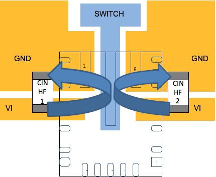
Figure 2: Placement of high-frequency CIN capacitors
In addition, by constructing the package in a certain manner, it is possible to remove the parasitic loop inductance and capacitance inside the package and reduce the switch-node ringing, which is a major contributor to the generation of noise (see Figure 3). The idea is that if you can reduce noise at the source, then you don’t need to tackle problems caused by additional components.

Figure 3: Switch node of the LM53635-Q1
Another technique for reducing noise in the system is called spread spectrum, which modulates the central switching frequency (in this case 2.1MHz) and suppresses the harmonics and sub-harmonics. Spread spectrum is very effective for reducing the overall noise peaks but will not influence the noise floor due to the spreading of the noise, as the name suggests. However, because spread spectrum helps with high-frequency harmonics, it can help meet the often-tough original equipment manufacturer (OEM) standards for EMI, make printed circuit board (PCB) designs simpler, and reduce filtering component size and cost.
Figure 4 shows the LM53635-Q1 in the 30MHz to 108MHz frequency band, with the spread spectrum turned off (left side) and turned on (right side).
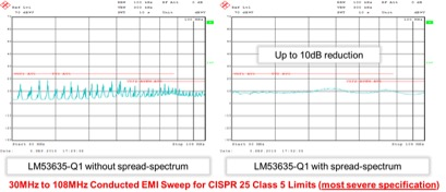
Figure 4: High Frequency harmonic suppression with spread spectrum
One of the major challenges to overcome is thermals due to space constraints and the ambient environment. A lot of automotive designs today are often incorporated into existing form factors and sizes used previously by mechanical functionality or just an empty space in the automotive design. A good example is the rearview mirror. In the past, rearview mirrors were simple hand-operated devices, but increasingly we are seeing the integration of electronics to accommodate new features like cameras. Given the radiated heat from the sun and also the material encasing of the mirrors (often plastics), the electronics can reach temperatures as high as 105°C on the PCB. The power supply has to be small enough to manage the integration of the electronics, but it also has to be highly efficient so that it doesn’t cause self-heating. TI designed the LM53635-Q1 to support high efficiency to minimise losses and also operate 2.1MHz to make the additional components needed to make the power supply as small as possible to manage the thermals and size. See Figure 5.

Figure 5: LM53635-Q1 efficiency operating at 2.1MHz
Maintaining quality is critical for automotive designs, even more so when designing for safety-based systems. Solderability is often a piece of the reliability puzzle. To enhance the quality of the soldering joint, you can use several techniques; one of these is wettable flanks. See Figure 6. Wettable flanks is a process of cutting a cavity in the edge of the package to enable more visible wetting of the side of the pins for optical inspection. This is helpful, as it eliminates the need for x-raying of the package to ensure adequate soldering, while also ensuring joint integrity.

Figure 6: Wettable flanks used on LM53635-Q1
As I have highlighted in this blog, there is much to consider when designing an automotive power supply as well as what additional functionality to add to your design to make the challenges more manageable. By understanding these, the end result can be a faster design, smaller solution and lower cost of ownership. Watch a video that demonstrates how to solve automotive EMI, thermal and system challenges with TI’s LM53635-Q1.