 As consumers demand affordable electronic products which are lighter, faster, more intelligent, more wearable and more multifunctional than ever before, packaging manufacturers continually develop components to meet these demands and the manufacturing world is forced into developing processes, and supply chains in order to keep up. Component development leads and manufacturing process follows, this has and continues to be, the process cycle of electronics development. Les Browne, Chemigraphic Ltd, outsourced EMS partner for OEMs, explains
With lead times being squeezed in the race to produce market-first products, NPI engineers are challenged with developing tighter than ever controls and processes in order to deliver products which not only satisfy quality, function and robustness, but also speed to market.
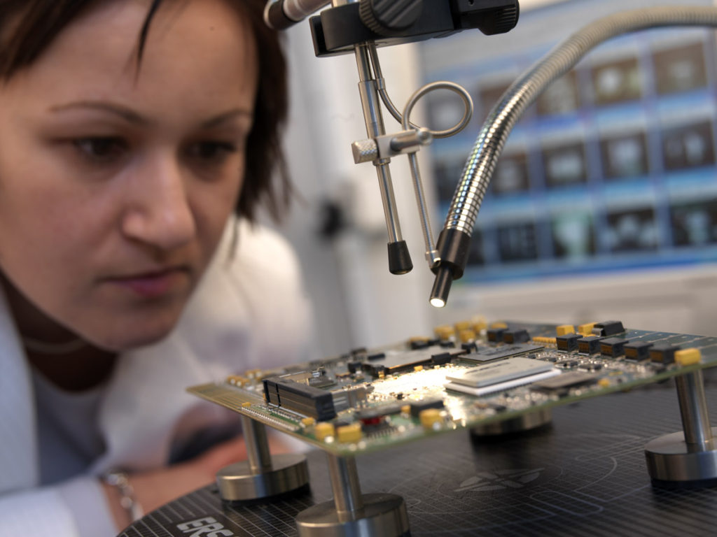
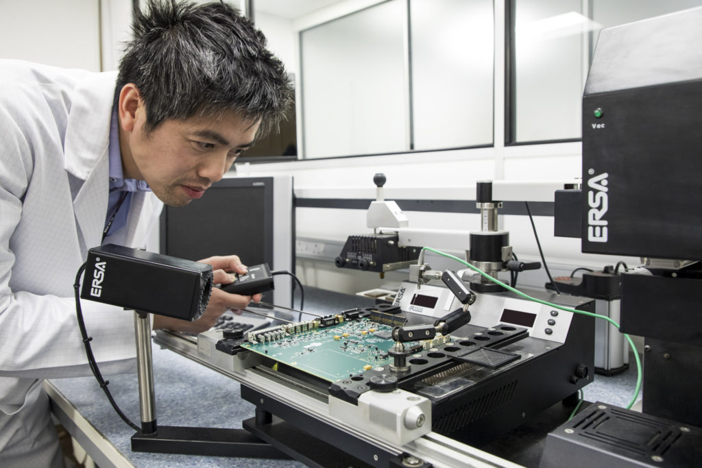
For Contract Electronic Manufacturers (CEMs), working with PCB manufacturers on developing PCBs for these products has become an essential part of the development process, in order to meet both technical as well as logistical challenges. In addition to having to source components and materials to meet shorter timeframes, these smaller and lighter products call for expert engineering in order to address spatial constraints and thermal management.
However, it’s also a very exciting time for PCB manufacturers and assembly houses. The proliferation of multi-functional and intelligent products means that new PCB technologies and applications are being continuously developed, as are process capabilities required to handle these sometimes tiny components and PCBs. Also increasing in sophistication is automation as a key element of leading assembly houses.
These are some of the impressive advances being made in PCB technology to meet the growing demands of OEMs and consumers in today’s hyper-connected world:
Modular Interconnect Devices (MID)
For tiny, lightweight devices such as hearing aids, pacemakers or medical implants, MIDs are ideal, as they:
- Utilise product housing and mechanical structures to carry electrical/electronic functionality
- Are modular so reduce assembly time and increase efficiency
- Provide more space for additional functionality
- Reduced in size, easily implanted and less offensive (aesthetically)
- Were initially developed for automotive mechanical switches and light clusters.
 Microfluidics, Lab on a Chip (LOC)
Now using PCB technology as a low cost solution to more expensive silicon manufacture:
- LOC is a millimetre sized PCB that integrates one or a number of laboratory functions
- Liquid carrying channels and electrical dams/switches are encapsulated within the PCB
- Developed as a result of PCB laser/plasma micro-via ablation and silk-screen technology
- Miniaturising chemical reactions amplifies results in order to aid more accurate analysis
- As a result of PCB technology OEM consumer products are safe to use and low cost
- Consumers are able to conduct medical and pharmaceutical monitoring testing at home.
 Planar PCBs, the next generation of PCB manufacture
The principal of PCB manufacturing has not changed since its inception. The process is subtractive and lithographic, though an alternative technology was developed in the late 70s (Planar), it proved to be too expensive over conventional ‘print and etch’ PCB manufacturing. The ‘Planar’ process produces glass flat PCBs (no copper track topography whatsoever), also without micro-feature constraints (track-and-gap). In addition, the technology produces solid copper vias increasing PCB thermal robustness.
The majority of challenges faced by CEMs today are around component placement, more so with the development of surface mount and Ball Grid Array components (BGA), and PCB flatness and topography, with Planar PCBs, none of this is a consideration:
- In appearance they look like conventional PCBs
- Originally developed by photocopier manufacturers
- Developed to make print-head components smaller and more thermally efficient
- The process of producing Planar PCBs using standalone automation is currently under development by a UK consortium, and is likely to be sold under licence to PCB producers.
 The future, growing organic biological circuits and components
This technology is at the cutting edge of electronics development, and will be used for medical implant, AI and supercomputing:
- These are organic semiconductors that grow in ordered structures
- Currently being developed by companies such as Philips Research
- The benefits to mankind are without question.


