Industry forecasts suggest that we’ll soon see tens of billions of things, from nannycams through bridge strain sensors to entire aircraft, connected to an ‘Internet of Things’ through which they will report data and take instructions. Many of these ‘smart objects’ will be functionally simple but expected to operate for months or even years without physical intervention. Others will be more complex, acting as gateways and aggregation points for data from devices on local sub-networks. Andrea Dodini, European marketing manager, Keysight Technologies, talks about the five common challenges designers face when developing these smart objects
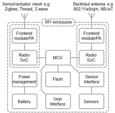 Increasing integration
Advances in mixed-signal IC technology are enabling smaller and lower-energy devices to be built that offer better performance and lower cost than discrete alternatives. These advantages come at the cost of design complexity, as digital, analogue and RF functions are co-designed and co-verified on one substrate. The complexity is worth it, though: early examples, such as low-power microcontrollers with integrated wireless links and interfaces for sensors and actuators, are already proving popular in IoT applications.
Another way of increasing integration is to print an antenna on the device’s circuit board, rather than using chip or external antennae. Even simple IoT devices may have multiple antennae (think WiFi and Bluetooth, for internet and local connectivity), and multiple radios driving them. It’s therefore important to be able to model and measure factors such as antenna match, efficiency, radiation, reception patterns and mutual interference in real-world situations.
Battery life
If you’re going to deploy a large network of sensor nodes, they’ll need long battery lives to limit the cost of maintaining them. Many IoT designers use strategies such as very low duty cycles and the implementation of various idle and sleep modes to cut energy use.
In higher-performance devices, the processor, display and wireless interfaces account for a lot of the energy budget. Understanding how energy is used by these devices means modelling the interaction of their subsystems, with each other and with their power-management strategies. This means understanding how much current each operating mode draws, and for how long. The challenge here is to measure currents that could range from nanoamps in sleep mode through to tenths of amps when active.
The operating lifetimes of unattended devices are being extended using new battery technologies, energy harvesting, low-power circuit design and lower energy communications strategies. Understanding how these variables affect device lifetimes and thermal requirements demands systematic energy analysis, which can then be used to take into account real-life environmental and network conditions when making hardware and software design decisions.
 Clean signals, clean power
Clean signals and clean power supplies are vital to the reliable long-term operation of any device. Signal and power integrity issues are especially important in circuits running at low voltages or high clock frequencies, where there is less tolerance for crosstalk.
There are four signal-integrity (SI) issues, relating to: a single net; coupling between multiple nets; power and ground paths in power distribution networks (PDN); and electromagnetic interference. These can be addressed by maintaining controlled impedances through interconnects, spacing circuit traces to reduce coupling, keeping return paths short, minimising PDN impedance, and good grounding and shielding.
Power integrity (PI) analysis considers how effectively power is converted and delivered from source to load. In low-power electronics, the tolerance on DC supply voltages is just +/-1 per cent. Any ripple, noise or transients on supply rails operating to such tight tolerances can affect clock and data signals and so the challenge is to measure ever smaller and faster AC signals on these rails.
 The many-radio problem
Many wireless technologies are being used in IoT devices. A battery-powered sensor may use a low duty-cycle, short-range wireless connection, while autonomous vehicles may need high-bandwidth, high-reliability links. This variety of standards presents a measurement challenge, since each may have different RF testing requirements and physical layers, supporting multiple modulation standards.
Developers also need to verify that devices interoperate correctly and can handle multiple standards concurrently, and this is where multi-standard test equipment can cut costs.
Interference, compliance and conformance
If tens of billions of IoT devices are deployed, they’ll have to share scarce resources such as the increasingly crowded unlicensed ISM radio band.
Designers must ensure their implementations can operate effectively in such dense signal environments, and meet network standards and regulatory requirements so they don’t cause co-channel or adjacent-channel interference.
IoT devices will also have to be checked for electromagnetic compatibility, through radiated and conducted emissions testing, and radiated and conducted immunity testing. To meet compliance certification measurements, testing tools will have to comply with the respective standards.
 Some solutions – design
Keysight EEsof’s EDA tools and design flows operate at the system, component and physical level to enable the kind of systemic simulations necessary for effective IoT device design.
SystemVue is an electronic system level design tool that enables system architects and algorithm developers to try various approaches to implementing the PHY layer of wireless communications systems, and includes virtual measurement tools to predict system performance.
Advanced Design System (ADS) enables co-design of ICs, packages and boards, so that circuits designed in multiple technologies can be simulated at both the circuit and full 3D electromagnetic (EM) level. The tool offers access to 3D planar and full 3D EM field solvers, and electro-thermal analysis. It also has a real-time optimisation cockpit, and libraries for the latest wireless standards.
SI analysis is supported with AC and S-parameter simulators, which compute the noise generated by each element in a circuit and then determine how it affects the network. ADS also offers SIPro, for EM characterisation of high-speed links on dense PCBs, and PIPro to analyse DC IR drop, AC impedance, and power-plane resonance.
 Some solutions – measurement
For battery current-drain analysis, Keysight offers the N6781A and N6786A two-quadrant source measurement units (SMUs), which have seamless ranging across seven decades to measure dynamic current drain signals. They can also emulate real batteries, and include zero-burden ammeters and voltmeters for run-down testing.
Keysight offers SI and PI measurement tools that can help validate simulation results. The ENA Option TDR addresses interconnect test, the Infiniium oscilloscopes support transmitter test, and the Bit Error Ratio Test (BERT) solutions can be used for receiver test.
For those developing IoT devices with wireless interfaces, Keysight offers benchtop, modular and one-box testers that can be updated with software and share a common approach to measurement that helps ensure a consistent and comparable measurement scheme from R&D to manufacturing.
Keysight’s Signal Studio software enables the creation of custom and standards-compliant waveforms, while the X-Series measurement applications enable one-button testing for the various IoT wireless formats. There’s also the 89600 VSA software for digital modulation analysis and troubleshooting.
Keysight also has dedicated equipment, such as the N9320B/N9322C Basic Spectrum Analyser for testing low-cost Bluetooth and Zigbee devices and modules, and the T3111S RIDER NFC Conformance Test System for testing NFC, EMV and ISO devices.
Conclusions
The IoT will be built with a broad variety of devices, from simple sensor nodes through to complex gateways. Despite the diversity of these devices, designers face some common challenges: minimising power consumption, maximising operating life, controlling the effects of interference and ensuring standards compliance. Using design and simulation tools that address these issues holistically, and which integrate with dedicated measurement tools, will increase designers’ chances of success considerably.


