 The world of technology is continually evolving and electronic devices are getting smaller, faster and smarter than ever before. As demand increases, not just in the mobile and smart phone market, but in aerospace, defence and medical, the need for Package on Package (PoP) technology in PCBs is increasingly important.
The original demand for package-on-package (PoP) technology when first introduced was to address the growing need to integrate logic and memory for advanced mobile phone platforms that are found in high-end mobile handsets and smart phones. PoP solutions over the last two years have also been finding their way into other mobile Internet devices and portable media players.
It doesn’t stop here, as the PoP solutions have also become the engine supporting the ever-increasing complexity and features required for devices in the medical industry. Simple medical procedures such as checking blood pressure and cholesterol levels have previously meant a visit to the GP or hospital. Now technological advances in PoP have helped the development of small hand-held diagnostic devices that patients can use in their own homes and demand for such devices is growing rapidly.
The PoP configuration has many other potential applications, including handheld point-of-sale devices, office equipment, high-end scientific instruments or even battlefield communications devices.
Broader applications for PoP technology see it enabling high-performance System-on-Module units containing processor and memory subsystems, input-output units, and communications.
These compact, fully-contained processing engines can be plugged into larger systems and have the advantage of modularity and scalability.
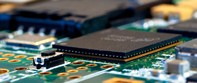
POP technology itself involves stacking semiconductor components on top of each other, rather than the traditional method of placing them side by side on the board, thereby reducing circuitry and board space required by up to 43%, and allowing the flexible addition of memory chips to compact devices without adding to the bulk of the product, or escalating production costs.
Currently in the UK, the industry standard and most common practice, is the implementation of two-stack semiconductor components (arranged with a standard interface to route signals between them). This allows higher component density in devices. Yet the implementation of two stack PoP technologies in UK manufacturing, despite improving, still isn’t being adopted and utilised as quickly as the industry foresaw it would.
For the bottom PoP package, the transition from wire bond to flip-chip is happening at a reasonable pace. As the need for smaller package size is driving finer ball pitch, and 0.4 mm ball pitch on the bottom PoP is now much more common place.
Meanwhile, the need for higher-speed and higher bandwidth DRAM, and DRAM with flash memory in the top package is driving the need for higher ball count for the top package. Higher ball counts and reduced package size requirements are necessitating finer ball pitch for the top package. Whereas 0.65 mm pitch may have been adequate in the past, now 0.5 mm pitch is required, and 0.4 mm pitch is on the horizon. This reduction in the package-to-package ball pitch has many implications. Finer pitch translates to smaller solder ball sizes and stand-off height of the top package after reflow on top of the bottom package. This will of course, affect the height allowance for the device housed in the bottom package.
In the Far East, in particular Japan, manufacturers are ahead of the game and have been implementing the next generation of PoP technologies, the three and four stacks, for several years.
Following hard on the heels of the Japanese manufacturers is Axiom. With the equipment, capability and experience of creating the two stacks, three and four stacks are a natural progression.
However, for the two-stack technology to become common practice, and the development of three and four stack technology to progress, investment in new technologies will be crucial.
Axiom has made this investment. It is still currently one of only a handful of UK contract electronic manufacturers incorporating PoP technology into its products. It has a state-of-the-art Fuji AIM Surface Mount Technology (SMT) machine which can place PoP components at a rate of eight seconds per device.
The use of this technology results in shorter device-to-device interconnects resulting in shorter signal paths, helping to improve connectivity; reduce EMC emissions and enabling manufacturers to make smaller, faster-reacting hand-held products.
Yet having the best available equipment is only part of the equation. The real competitive advantage is the skills, techniques and knowledge associated with making the most of the technology. This, in turn provides customers with the best solutions.
That said, PoP technology is not without manufacturing challenges. PCB manufacturers that produce the bare circuit boards are still finding it challenging to the get the solder mask alignment correct for PoP printed circuit boards. This means that some batches are being rejected as not being suitable for use. On 0.4mm pitch devices in particular, the pitch of the solder balls are so close together that any misalignment will cause major shorting on the bottom stack.
One of the major challenges faced when placing such small components is achieving consistent print and release of solder paste onto tiny PCB pads. This issue can be solved through a combination of advanced stencil design, deployment of appropriate solder paste and dedicated under-board support for both PCB printing and component placement.
The team at Axiom has worked to characterise the assembly process by experimenting with a variety of different solder pastes and tack fluxes to bond the stacked components together, as well as soldering the base package to the PCB. They have settled on a solder paste printed base package followed by a solder paste dipped upper package; before reflowing the entire assembly to achieve the finished solder joint connections.
By thoroughly inspecting each method ,for evidence of satisfactory solder joints, the team has tailored and perfected the process, investing in a DAGE 7600 XiDAT digital X-Ray inspection system capable of inspecting multi-level BGAs and enabling the most effective quality inspection of final products.
Despite all the manufacturing challenges, there is no doubt that the current generation of PoP technologies will continue to see strong growth within the UK with the potential of opening up new market sectors. In order for the industry to fully realise its potential and meet the complex set of next-generation PoP requirements, a new higher density bottom package that is readily available, will be crucial.
Rob Taylor is Senior Engineer at Axiom Manufacturing Services
