Industrial Imaging is a growing market covering applications that range from inspection and robot guidance to high-end surveillance, intelligent transportation systems, scientific research, and much more. While customers working in these applications will all agree they require a “high performance” imaging system, the varying needs of these different applications means that the specific imaging requirements can vary greatly depending on the application being addressed. Michael DeLuca, Go To Market Manager, Industrial Solutions Division, ON Semiconductor, explains
Sometimes, “high performance” might mean capturing a high resolution image with high frame rate – capturing multiple megapixels at 50, or 100, or 200 frames per second or more. But other times, different performance features might be more important, such as a physical small camera footprint, enhanced light sensitivity (whether visible or near-infrared), colour fidelity, or customisability. With the breadth of this application space, no single imaging solution can effectively be used to meet all of these needs, requiring camera manufacturers to provide a portfolio of different cameras, each with different resolutions, frame rates, light sensitivities, output interfaces, and more, to effectively serve this market. And to be competitive, this portfolio needs to be developed in a cost effective manner, allowing multiple camera models to be designed, manufactured, and supported as quickly and efficiently as possible.
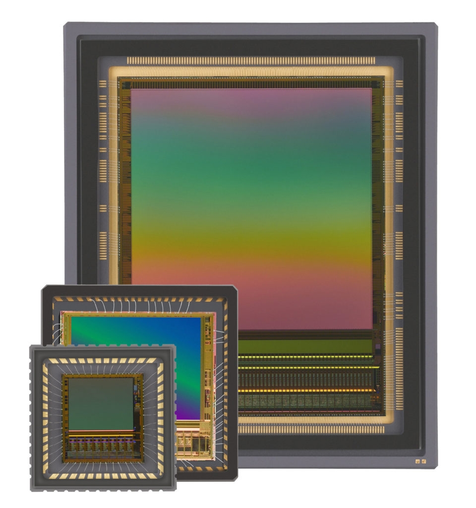
Image sensor manufacturers can simplify development of this type of camera portfolio by developing an integrated family of high performance image sensors that span a range of resolutions and configuration options and that is based on a common image sensor architecture. By designing for such a platform, camera manufacturers can easily leverage a single camera design to support the entire family of image sensors.
One example of this type of platform design for image sensors can be found in ON Semiconductor’s PYTHON family of global shutter CMOS image sensors. Since the VGA, 0.5 megapixel, and 1.3 megapixel members of the family all share a common package with the same pin definitions and electrical connections, a single camera can be easily designed to support all three of these devices. In a similar way, one design can support both the 2 and 5 megapixel members of the family as well. But in practice these two board layouts can be combined into one, since a socket is available that supports both of the LCC packages used in these devices. This allows devices from the VGA to 5 megapixels to be supported using a single board layout. When adding a second board design for the µPGA high resolution devices, all nine resolutions in the family – corresponding to 36 different saleable cameras in monochrome, colour, and extended NIR configurations – can be supported using only two PCBs. This design commonality greatly simplifies the work needed by camera manufacturers to develop the broad range of camera options needed for industrial imaging applications, lowering costs and accelerating time-to-market for new camera designs.
Even with this type of inter-compatibility, of course, the actual imaging performance of the devices must meet the needs of the targeted applications. Here, the latest CMOS design and manufacturing technologies are required to enable global shutter imaging for the capture of moving objects without the introduction of motion artifacts, while still providing the high sensitivity and low noise needed to preserve the integrity of the final image even as lighting conditions are reduced. Ideally, image capture will span a broad range of different wavelengths, including designs to provide enhanced near-infrared sensitivity for applications where detection of long wavelength light, such as 850 nm or beyond, can be critical.
Data bandwidth can also be a critical performance parameter, as end users look not only to optimise frame rates for their application but also to maximise utilisation of established camera interfaces. Interfaces such as 10 GigE, USB 3.1, and CoaXpress are now widely adopted, and image sensor platforms that match or exceed the bandwidths associated with these interfaces provide camera manufacturers and end users additional flexibility in the deployment of imaging systems.

PYTHON devices provide a good example of this type of image sensor design, with the highest resolution members of the family incorporating 32 separate, high speed LVDS output channels. This results in a data throughput of 20 gigabits per second – well above the effective bandwidth available from interfaces such as USB 3.1 or 10 GigE. In addition, the actual frame rate available from devices in the family can be increased, if needed, by reading out only a portion of the imaging array (a region of interest, or ROI). These devices support up to 32 separate ROIs that are configurable frame to frame, simplifying the work needed to monitor or track an object or a person as they move across the full field of view of the camera. This means, for example, that the PYTHON 25k can read out a 1080p resolution window at over 400 fps if needed, which is twice the frame rate available from the PYTHON 2000 for the same 1080p resolution.
To truly maximise the power of a platform design for an image sensor family, multiple product configurations – such as the 65 different orderable devices available in the PYTHON family – need to be available to allow camera manufacturers to select the right resolution, colour configuration, power requirements, output speeds, and packaging configuration needed for a given application. And then a variety of different support options need to be available to help not only in the evaluation of the devices but also as a reference while a new design is underway. Detailed datasheets provide information on the performance of the devices before starting a new design, and evaluation kits allow the full performance of an image sensor to be evaluated on site. And then once a design is started, these same documents and tools can be used as a reference to assist with debugging and optimisation – helping to make sure the new camera design provides the best performance possible.
With the explosion of opportunities becoming available in industrial imaging applications, the use of a platform design – not only for the design and manufacture of cameras but also the image sensors used in them – becomes even more important as a way to provide the variety of imaging options required in these applications. By enabling camera development to be leveraged across a full product line of image sensors with multiple configurations and resolutions, camera manufacturers can simplify the work needed to develop, design, and then support a full range of cameras that provide the critical imaging performance needed by their customers.


