 Diodes Incorporated is providing smartphone and tablet designs with an alternative to miniature DFN0603 devices with the introduction of its first wafer level chip scale packaged Schottky, that offers twice the power density for the same PCB footprint.
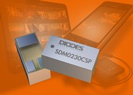
In the X3-WLCUS0603-3 solder pad package, the 30V, 0.2A SDM0230CSP Schottky diode has a typical thermal resistance of just 261ºC/W. This is around half that of the DFN0603 package so power dissipation is doubled in switching, reverse-blocking and rectification circuits.
Using 70% less board space than the industry-standard DFN1006 and SOD923 packaged Schottkys, the 0.18mm2 footprint SDM0230CSP is also well suited to high-density design. Additionally, its 0.3mm off-board profile is 25% thinner, benefiting ultra-thin portable products.
The Schottky’s low maximum forward voltage of just 0.5V for a forward current of 0.2A, combined with a typical low leakage current of only 1.5mA at a reverse voltage of 30V, means it minimises power losses, thus extending battery life.