 Back in 1999, when the very first NAND storage was developed, flash memory was based on a sizable design rule of 120 nanometers. As storage technology has evolved, this design rule has reduced significantly in size, ultimately reaching as little as 10nanometers. As a result of this reduction, designers have been able to produce a NAND flash memory device with 64 times as many cells as those developed a mere 15 years ago.
We are now at a stage where a typical 1x nanometer 128Gb 3Gb MLC device contains more than 43 billion NAND cells – enough to store 16GB of data. This increased storage however does not come without its costs.
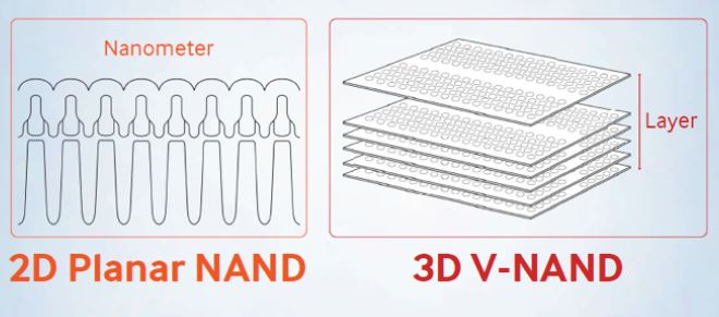
For the past 40 years, conventional flash memory has been based on two-dimensional planar structures that make use of floating gate transistors. These structures consisted of billions of cells organised into flat rows, pushed together in an effort to minimise the size of the end device. As manufacturers move beyond this point however, they have grown increasingly aware of the possibility of reaching a “scaling limit”.
As we approach the 10 nanometer class and beyond, the space between cells decreases. As a result, the cells begin to affect each other’s behaviors via a coupling effect – an unintended energy exchange resulting in damage to the device or even data corruption. Once this scaling limit is reached, manufacturers will no longer be able to shrink their devices down without jeopardising the integrity of their cells.
In the past, when cells had a design rule of 30 nanometers or more, these problems were easily controlled or worked out via the design effort. Now however, as the size of the design rule decreases, the ability to solve such problems becomes ever more complicated, running a higher risk of data corruption.
In addition to the challenges of interference, the shrinking of NAND cells also leads to growing difficulties in the photolithography process. As the design rule gets lower, it becomes increasingly difficult to find an appropriate light source. As an example, the light source for a 40 nanometer class design rule can be used to inscribe photo mask patterning on a NAND wafer without any issue. Once the design approaches 1x nanometer however, this light source cannot penetrate the smaller pattern. As a result, the development of adequate photolithography for 1x nanometer patterning requires significant technological investment.
3D V-NAND – Starting from the ground up
As the possibility of a NAND scaling limit grew increasingly possible, research and development teams around the world begun working to develop a potential solution.
Within Samsung, our approach involved a completely new “ground-up” structure that adopted the concept of “layers” instead of nanometers. In conventional flash storage, memory is based on two-dimensional planar structures that make use of floating gate transistors. These structures consist of billions of cells organised into flat rows, pushed together in an effort to minimise the size of the end device.
As an alternative to this forty year-old layout, we decided that – rather than squeezing more cells into the same horizontal space – we should look to build vertically on top of the existing planar structure.
This decision was made following the conception of a simple analogy, which compared living in a house with living in an apartment building. Where once a two-story home could only house four people, the introduction of apartment blocks meant that hundreds more people could be housed in the exact same landmass, without reducing the overall size of their living conditions. This allows the inhabitants of an apartment to occupy the same amount of room without interfering in each other’s personal space.
By layering cells on top of one another Samsung was able to apply this analogy to their NAND memory, building vertically to create the new “V-NAND” (Vertical NAND) structures. While this development started with a mere 24 vertical layers, technological advancements have allowed us to increase this amount to 32 layers. As a result, the technology has now moved beyond a 2D planar structure and into the third dimension – thus, 3D VNAND.
This new structure not only provides benefits relating to size, it is also improving the endurance of each individual cell. If a cell’s usage is write intensive, then users will see up to a 5-fold improvement in the longevity of their device. If on the other hand it is read-centric, users can expect to see up to a 10-fold improvement in endurance. Additionally, Samsung has been able to demonstrate up to an 100% increase in write speed, helping to lower energy consumption and save on future maintenance costs.
While the idea of moving from the horizontal to the vertical planar sounds simple enough, it has actually taken almost a decade to develop a structure that works. One of the biggest challenges facing this new development was the decision of which material to use. Whereas most memory uses conductors, allowing the charge to move freely through floating gates, V-NAND requires a more solid insulator. This insulator however, cannot move at the pace of a viscous conductor. In an effort to solve this problem, Samsung returned to an 8-year old technology – Charge Trap Flash (CTF). By revising CTF’s cylinder-shaped architecture, Samsung was able to develop a system in which electrical charges could be temporarily placed in a silicon nitride (SiN) holding chamber until needed. This new technique was used as an alternative to traditional floating gates, helping prevent further interference between the neighboring cells.
Overcoming these challenges did not come cheap. With a capable fab in excess of $11bn and the registration of over 300 patents, 3D VNAND has proved a colossal development for Samsung’s Green Memory division. However, as a result of this early-stage investment, Samsung remains the only memory manufacturer currently offering vertical NAND technology. A unique competitive position that seems unlikely to change in the near future.
As data centers increase their capacity and the amount of data in existence continues to grow, the benefits of this position cannot be understated in the memory market.
Thomas Arenz, head of MI, SBD and marketing communications EMEA at Samsung Semiconductor


